- Document my progress and serve as high-level documentation for the project
- Serve as an introductory resource for people trying to gain an understanding of all levels of the Ethernet stack
In this post
In part 0 I will begin by breaking down the testing setup and a quick overview of the components we will need to implement to start receiving packets on the other end of the link.
Testing Setup
In order to keep cost down and implementation complexity low we are going to start by brining up 10Gb ethernet and then later upgrading it to 25Gb. The first and most obvious component we need is the FPGA board itself. Since I can’t drop over $1,000 on a dev board as a college student we will be using the Alibaba Cloud FPGA board which can be had for $150 on ebay. Some information on this board can be found here. The board has an exposed JTAG port so we will also need a programmer. For this we will be using a knockoff waveshare platform cable from amazon that can be found here. Using this cable allows us to use the Vivado tools such as VIO and ILA for debugging. In addition to the FPGA we will need SFP transceivers, fiber cables and a 25Gb NIC.
Introduction to the parts of 10Gb Ethernet
This is going to be a short introduction to the components we will be implementing in the future parts of this series.
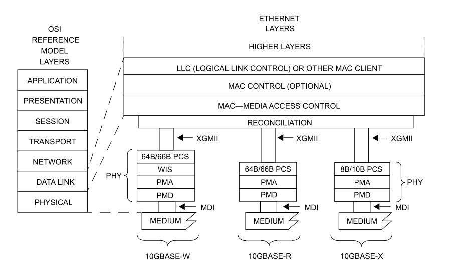
The above image is from the IEEE 802.3 Ethernet Specification (Figure 44–1—Architectural positioning of 10 Gigabit Ethernet) and details the different layers of the stack and how they are connected. We will be implementing 10GBASE-R which has from bottom to top the PMD, PMA, 65B/66B PCS, Reconciliation, and MAC
PMD (Physical Medium Dependent)
This layer is implemented by the SFP+ or SFP28 Transceiver and converts from an NRZ data stream for transmit and one for receive on the top to either Fiber or Copper on the bottom which is the Medium and MDI (Medium Dependent Interface)
PMA (Physical Medium Attachment)
They layer is implemented by that hard transceiver IP on the FGPA. In the case of the XCKU3P there are 16 GTY transceivers and we need one per SFP+/SFP28 port. This layer will be detailed in the next post.
64B/66B PCS (Physical Coding Sublayer)
This is the first layer in the stack that we need to implement ourselves. The main job of the PCS is to convert from XGMII (10 Gigabit Media Independent Interface) on top to the data bits that are actually sent over the wire.
Reconciliation
This is the next layer in the stack and one that we will roll into the MAC layer.
MAC (Media Access Control) + RS (Reconciliation)
The Media Access Control and Reconciliation sublayers convert from the upper layers of the OSI reference models to the the Data Link and Physical layers.
]]>