0 To 25Gb Ethernet: Part 1 The PMA
Make sure to read the previous post for an overview of what we will be talking about today:
- 0 To 25Gb Ethernet: Part 0
- 0 To 25Gb Ethernet: Part 1 The PMA (this post)
- 0 To 25Gb Ethernet: Part 2 The Scrambler
- 0 To 25Gb Ethernet: Part 3 The Encoder
What does the PMA Do?
In the ethernet specification Clause 51 subclause 51.1 we get the definition
“The purpose of the serial PMA is to attach the PMD of choice to its client, i.e., the PCS or WIS sublayer.”
I don’t know about you but this doesn’t help me very much so lets continue reading the specification of the PMA.
Later down we find that there is a list of a few functions that the PMA must do in either direction. In the transmit direction:
- Provide transmit source clock to PMA client.
- Serialization of 16-bit data to serial bit stream.
- Transmission of serial data to PMD.
In the receive direction:
- Bit clock recovery of serial data from PMD.
- Provide receive clock to PMA client.
- Deserialization of serial data to 16-bit parallel data.
- Transmission of parallel data to PMA client.
- Provide link status information.
So these tasks encompass generating the transmit clock, recovering the receive clock and converting between the serial interface to the PMD and the parallel interface of the PCS.
Implementing the PMA
First lets determine the serial bit rate the PMA needs to output and then the clock rate of the parallel interface.
For the serial interface we need to transmit 10GBit/s of data but we are using 64b/66b coding (covered in a later post) so we actually need to transmit at 10GBit * 66/64 = 10.3125 GBit/s
Looking at the datasheet for the XCKU3P chip we can see that it has 16 GTY Transceivers which support data rates up to 32.75 GBit/s so these will be perfect for our application.
Transceiver Example Project
In order to get familiar with the transceivers we will generate the IP and run the example project. The example project along with a loopback SFP+ module will allow us to test the transceivers, SPF cages and SPF modules.
Loopback SFP Module
You can buy specific loopback modules for this testing but for a cheaper option you can take a standard optical SFP+ module and a duplex LC cable and split the LC connector and put a single fiber into both sides of the connector so the TX side loops back into the RX side. This is now a loopback cable which we can use for testing.
Generating the GTY Transceiver IP
General Settings
In the Vivado IP Catalog search for the “Ultrascale FPGAs Transceiver Wizard” and open the customization wizard. First we should select the “GTY: 10GBASE-R” configuration preset which will the settings in as below
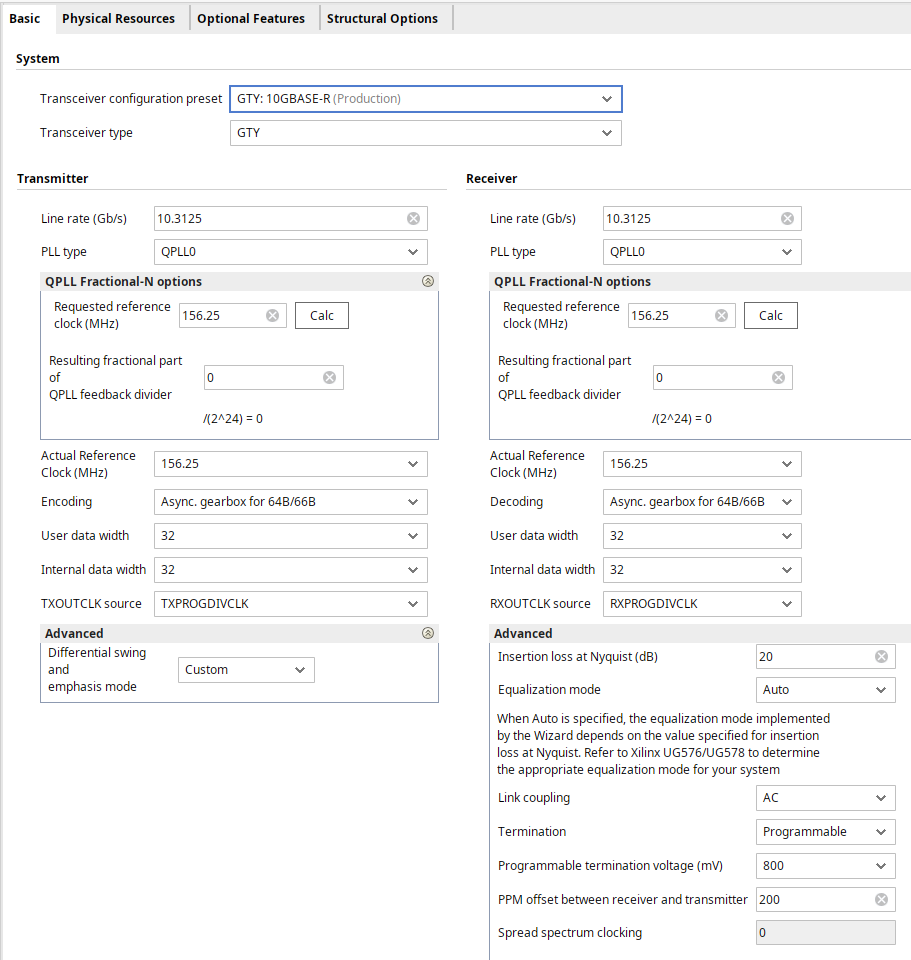
Now lets go over some of the settings that this preset selects so we can better understand the settings we are choosing.
- Line rate
As we saw above the true line rate is 10.3125 which was properly filled into both the transmitter and receiver.
- Actual Reference Clock (MHz)
This is the frequency of the reference oscillator on the circuit board and comes from the datasheet or XDC file of our specific board but in most cases it should be 156.25 MHz.
- Encoding
The default here is “Async. gearbox for 64B/66B” which is the easiest option to get started and will be covered in much more depth later in the series. For now the important part to know about this encoding option is that for every block it will take in 64 bits of data and two bits of header. The gearbox will then handle crossing into the XCLK clock domain.
- User data width, Internal data width
This is the amount of bits of data that will be transferred into or out of the transceiver every clock cycle.
Physical Resources
This setting depends on the development board you are using but on the Alibaba cloud accelerator the first SFP socket is connected to X0Y15 and the second is connected to X0Y14. You can check this in the pinout and match the RX and TX pins of the socket to the pins in the right most column of the selection.
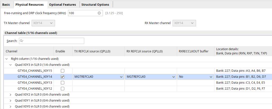
We also need to set the free-running clock frequency to the frequency of the other oscillator on our board which in our case is 100MHz.
Next we can leave the rest of the settings at their default values and generate the IP. After the IP is generated we want to find it in the sources window and right click and select “Open example project”. This will open the example project which needs a few minor changes before we can test it on the FPGA.
Board Specific Project Changes
The top level module sfp_gty_1_example_top has a few inputs and outputs that either need to be mapped to buttons and LEDs or removed. In our case we dont have a reset button and all the LEDs are under covers so we will just remove the connection. We also have a differential signal on our 100MHz clock
The default module declaration looks like this
module sfp_gty_1_example_top (

  // Differential reference clock inputs
  input  wire mgtrefclk0_x0y3_p,
  input  wire mgtrefclk0_x0y3_n,

  // Serial data ports for transceiver channel 0
  input  wire ch0_gtyrxn_in,
  input  wire ch0_gtyrxp_in,
  output wire ch0_gtytxn_out,
  output wire ch0_gtytxp_out,

  // User-provided ports for reset helper block(s)
  input  wire hb_gtwiz_reset_clk_freerun_in,
  input  wire hb_gtwiz_reset_all_in,

  // PRBS-based link status ports
  input  wire link_down_latched_reset_in,
  output wire link_status_out,
  output reg  link_down_latched_out = 1'b1

);
and we want to change it to this
module sfp_gty_1_example_top (

  // Differential reference clock inputs
  input  wire mgtrefclk0_x0y3_p,
  input  wire mgtrefclk0_x0y3_n,

  // Serial data ports for transceiver channel 0
  input  wire ch0_gtyrxn_in,
  input  wire ch0_gtyrxp_in,
  output wire ch0_gtytxn_out,
  output wire ch0_gtytxp_out,

  // User-provided ports for reset helper block(s)
  input  wire hb_gtwiz_reset_clk_freerun_in_p,
  input  wire hb_gtwiz_reset_clk_freerun_in_n
);

  wire hb_gtwiz_reset_all_in = 0;
  wire link_down_latched_reset_in = 0;
  wire link_status_out;
  reg link_down_latched_out = 1'b1;
  wire hb_gtwiz_reset_clk_freerun_in;

  IBUFDS #(
    .DIFF_TERM("TRUE"),
    .IOSTANDARD("LVDS")
  ) m_ibufds (
    .I(hb_gtwiz_reset_clk_freerun_in_p),
    .IB(hb_gtwiz_reset_clk_freerun_in_n),
    .O(hb_gtwiz_reset_clk_freerun_in)
  );
We also need to map the freerun clock ports to the pins in the constraints file. This is pretty easy by adding these two lines in the xdc file
set_property -dict {LOC E18  IOSTANDARD LVDS} [get_ports {hb_gtwiz_reset_clk_freerun_in_p}]
set_property -dict {LOC D18  IOSTANDARD LVDS} [get_ports {hb_gtwiz_reset_clk_freerun_in_n}]
we then change this line in the xdc
create_clock -name clk_freerun -period 10.0 [get_ports hb_gtwiz_reset_clk_freerun_in]
to this
create_clock -name clk_freerun -period 10.0 [get_ports hb_gtwiz_reset_clk_freerun_in_p]
Running the Example Project
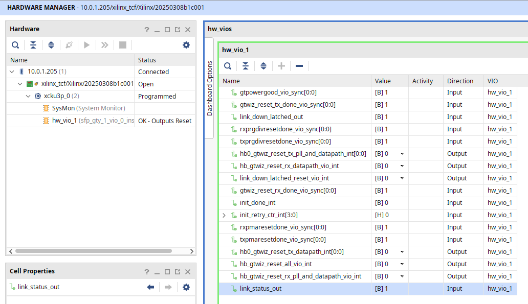
Now we can press Generate Bitstream on the bottom left of the Vivado window. This will run through all the steps of the Synthesis and Implementation flow. After the Bitsream is complete we can open the hardware manager and program the FPGA. After programming we can connect our loopback cable into the bottom port and then in the VIO we can see that link_status_out=1 If you dont see this make sure your loopback cable is plugged into the correct port.
Next Time
Now that we have the transceiver IP working we will start working on getting our own components working around the IP. Next time we will be looking at the PCS and specifically the scrambler and descrambler.